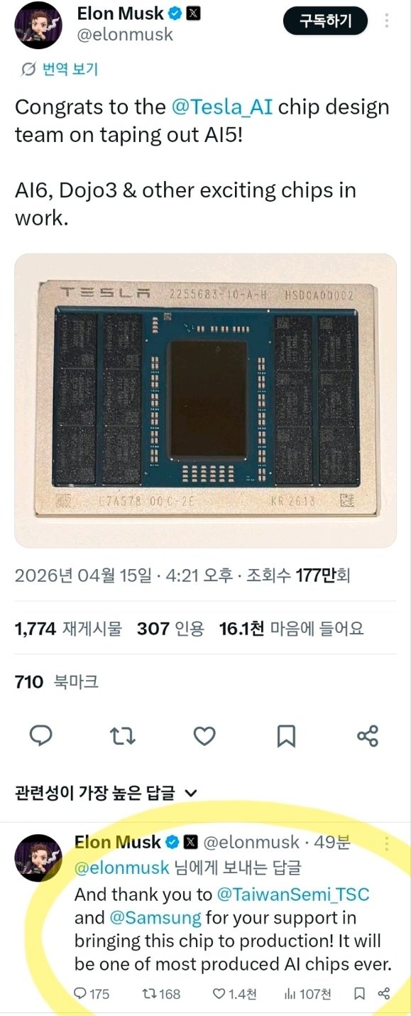

On the 15th (local time), the global semiconductor industry’s attention turned to a post on X (formerly Twitter) by Tesla CEO Elon Musk. The spotlight came as a congratulatory message announcing the tape-out (transfer to foundry after design completion) of Tesla’s next-generation artificial intelligence chip “AI5” was accompanied by a photo of the actual chip.
Industry observers noted two key facts. First was the incident where Musk, while thanking partners Samsung Electronics (005930.KS) and TSMC, accidentally tagged a Taiwanese company with a similar name (TSC) instead of industry leader TSMC (@TaiwanSemi_TSC). While this occurred because TSMC does not operate an official X account, the real focus was the second fact: the clearly engraved marking “KR2613” at the bottom of the chip.
KR2613: Produced at Korean Fab in Week 13 of This Year
This code indicates that the prototype was manufactured at Samsung Electronics’ foundry plant in Korea (KR) during week 13 of 2026 (late March to early April). Until now, Taiwan’s TSMC had virtually monopolized Tesla’s core autonomous driving semiconductor volumes. However, this prototype label signals to the industry that TSMC’s monopoly has cracked and Samsung Electronics has wedged itself into that gap.
Musk’s vision announced during Tesla’s third-quarter earnings call last October—that “the AI5 chip will be manufactured jointly by Samsung and TSMC”—has become reality. At that time, Musk highly praised Samsung’s Taylor, Texas plant infrastructure while hinting at plans to diversify production volumes.
Packed TSMC Lines Give Samsung Windfall
Market logic lies behind Tesla clasping hands with Samsung again. Currently, the global semiconductor market is experiencing severe bottlenecks at TSMC’s advanced processes due to exploding AI chip demand led by Nvidia. For Tesla, which needs massive volumes of AI chips to advance Full Self-Driving (FSD) and expand its Dojo supercomputer lineup, relying solely on TSMC poses too great a supply chain risk.
The assessment is that Samsung Electronics’ foundry division, which has steadily improved its technology while absorbing losses in the trillions of won, is finally seeing its capabilities shine. According to industry sources, Samsung’s 2-nanometer process has secured price competitiveness approximately 30% lower than TSMC. Additionally, Samsung deployed “SF2T,” a custom foundry process exclusively for Tesla. This tailored process, which Samsung had said at last year’s “SAFE 2025” forum was being developed for successor chips like the AI6, was preemptively applied starting with the AI5, creating a lock-in effect.
Too Early to Celebrate: Yield Improvements and Additional Customers Needed
However, the consensus is that it’s still too early to celebrate. Samsung, which struggled with low yields during the early introduction of Gate-All-Around (GAA) technology in its 3-nanometer process, is showing clear improvement with its 2-nanometer process. Yields that were below 50% as recently as the second half of last year have reportedly surged to above 50% recently. However, sources indicate this is still not sufficient to ensure profitability. Securing additional orders from big tech companies that had previously left Samsung is also cited as a challenge.
Meanwhile, although SK hynix memory was installed in the Tesla AI5 chip revealed this time, Samsung Electronics has also been identified as a joint supplier.
*”Gap World” is a column where reporter Seo Jong-“gap” delves into the gaps between news flooding the era of technology hegemony competition. Check “Gap World” for the core insights and outlook on cutting-edge technology and semiconductor issues. Please subscribe to the Gap World column and the reporter’s page.*